
When materials are made thinner and thinner, they undergo a remarkable transformation. Two-dimensional materials consisting of only one or two layers of molecules exhibit properties that differ significantly from their thicker counterparts. A team of researchers led by physicist Prof. Ursula Wurstbauer at the University of Münster is delving into the ways to control the properties of two-dimensional crystals. The goal is to manipulate these materials to behave like insulators, electrical conductors, superconductors, or ferromagnets, among other possibilities.
The key to achieving these different properties lies in understanding the interactions between the charge carriers (electrons) and the energy landscape of the crystals. By investigating these interactions, the team has successfully generated and quantitatively demonstrated collective excitations of the charge carriers within various energy landscapes. This groundbreaking study, published in Physical Review Letters, sheds light on the electronic characteristics of crystal structures and provides insights into how to influence them.
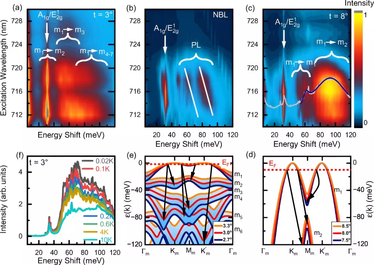
To induce the desired properties, the researchers stacked two layers of a two-dimensional crystal on top of each other and twisted them slightly. This twisting action creates moiré patterns, akin to the patterns formed by two layers of thin curtain fabric laid on top of each other. These moiré patterns define the energy landscape, causing the electrons to move at a much slower pace. As a result, the electrons engage in intensive interactions with each other, leading to what is known as strongly correlated behavior.
Drawing a comparison to the dance floor, Wurstbauer explains how electrons exhibit different behaviors in moiré patterns compared to standard dancing. The electrons’ movement within the patterns depends heavily on the specific pattern, the number of charge carriers present, and the resulting energy landscape. Just as dancers’ movements are influenced by the music and the dance floor, electrons’ behavior is dictated by the patterns and energy landscapes they encounter.
Potential Applications in Quantum Technology
The implications of these findings extend beyond basic research. The unique properties of these material systems have the potential to revolutionize quantum technology and facilitate the development of neuromorphic components and circuits. These innovative applications could pave the way for advancements in various fields, offering a glimpse into the future of technology.
Combining Experimental Work with Theoretical Analyses
The research team, comprised of scientists from multiple institutions, including the University of Hamburg, RWTH Aachen University, and the Max Planck Institute for the Structure and Dynamics of Matter in Hamburg, conducted a comprehensive study. They prepared different two-dimensional crystals such as graphene, molybdenum diselenide, and tungsten diselenide and analyzed them using optical spectroscopy methods at cryogenic temperatures, specifically resonant inelastic light scattering spectroscopy.
The study’s findings not only deepen our understanding of the properties of two-dimensional crystals but also open up new avenues for exploring their potential applications in cutting-edge technologies. By manipulating the interactions between charge carriers and energy landscapes, researchers have unlocked a world of possibilities in the realm of materials science and quantum technology.