
The field of quantum sensing has seen a significant breakthrough with the development of a new 2D quantum sensing chip by researchers at TMOS and RMIT University. Traditional quantum sensing chips have been made from diamond, known for its robustness. However, diamond-based sensors are limited in their ability to detect magnetic fields only when aligned in a specific direction. This limitation results in blind spots and the need for multiple sensors at varying alignments, making operation more complex and limiting versatility in different applications.
Innovative researchers led by Jean-Philippe Tetienne and Igor Aharonovich are pioneering a new quantum sensing platform using hexagonal boron nitride (hBN). Unlike diamond, hBN crystals are flexible and made up of atomically thick sheets, allowing the sensing chips to conform to the shape of the sample being studied. This flexibility enables the sensors to get much closer to samples than diamond-based sensors, enhancing their accuracy and efficiency.
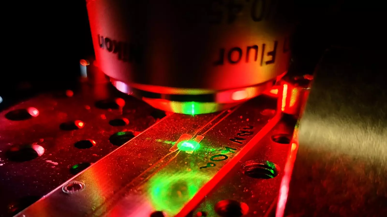
One of the key advancements in this new quantum sensing chip is the discovery of a carbon-based defect within hBN that can detect magnetic fields in any direction. Through a Rabi measurement experiment, researchers identified this defect as a spin half system, allowing for the sensor’s unique capability to detect magnetic fields without alignment restrictions. This defect can also be electrically controlled, similar to the well-understood boron vacancy defect in hBN, allowing for enhanced functionality and versatility in sensing applications.
The unique 2D form of hBN sensors offers a wide range of applications beyond traditional diamond-based sensors. These sensors can be used in biological systems as in-situ probes, offering directional independence and precise sensing capabilities. Additionally, hBN sensors are cost-effective and accessible, providing a more practical solution for quantum sensing technology compared to diamond.
The development of this new quantum sensing technology opens up a wide range of possibilities for future applications. From in-field identification of magnetic geological features to radio spectroscopy across a wider band, the spin half nature of the defect in hBN sensors offers unprecedented opportunities for quantum sensing. Further research into the atomic defects within hBN will lead to enhanced sensor devices with optimal performance, pushing the boundaries of quantum technology even further.
The new 2D quantum sensing chip developed by researchers at TMOS and RMIT University represents a significant advancement in the field of quantum sensing. By overcoming the limitations of diamond-based sensors and harnessing the unique properties of hBN, this technology opens up new possibilities for precise, versatile, and cost-effective quantum sensing applications. With continued research and development, the potential for quantum sensing technology to revolutionize various industries is on the horizon.