
Two-dimensional (2D) semiconducting materials have unique optoelectronic properties that have the potential to revolutionize the development of ultra-thin and tunable electronic components. However, despite their promising advantages over traditional bulk semiconductors, effectively integrating these materials with gate dielectrics has proven to be a challenging task. This has often resulted in the formation of interfacial traps that can significantly degrade the performance of transistors.
Researchers at King Abdullah University of Science and Technology (KAUST), Soochow University, and other global institutes have recently introduced a groundbreaking approach that could pave the way for the fabrication of high-performing transistors based on 2D semiconductors. In a paper published in Nature Electronics, they proposed a novel design that involves the use of hexagonal boron nitride (h-BN) dielectrics and metal gate electrodes with a high cohesive energy.
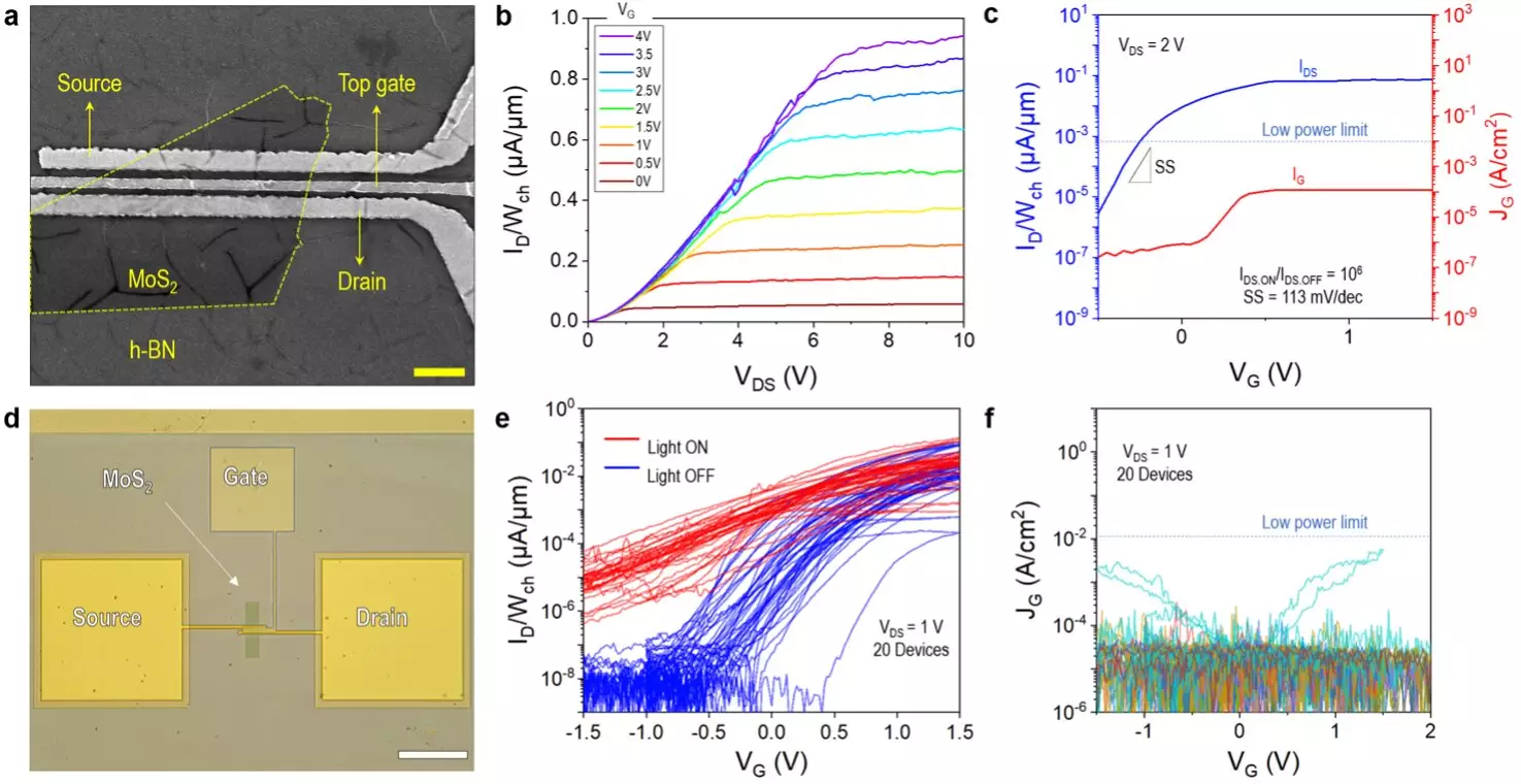
According to Yaqing Shen, the first author of the paper, the research team found that using platinum (Pt) as an anode resulted in a reduced likelihood of dielectric breakdown in the h-BN stack. Building upon this discovery, they conducted a series of experiments and determined that Pt/h-BN gate stacks exhibited a 500-times lower leakage current compared to Au/h-BN gate stacks. Additionally, they demonstrated a high dielectric strength of at least 25 MV/cm using this configuration.
Shen, Prof. Mario Lanza, and their collaborators successfully fabricated over 1,000 devices utilizing chemical vapor deposited h-BN as dielectrics. The researchers discovered that h-BN gate dielectrics were best compatible with high cohesive energy metals, such as Pt and tungsten (W). The fabrication process involved the precise patterning of source and drain electrodes on a SiO2/Si substrate, the transfer of MoS2 onto these electrodes to form the channel, and the use of CVD h-BN film as the gate dielectric.
In the final steps of the transistor fabrication process, the team patterned the Pt gate electrode using electron beam lithography and deposited it via e-beam evaporation. The clean van der Waals interface between MoS2 and h-BN in their transistors significantly improved reliability and performance by minimizing defects and enhancing gate control. Contrary to popular belief, the researchers demonstrated that by selecting the appropriate metal electrodes, CVD h-BN could effectively serve as a gate dielectric in 2D transistors.
Potential Impact and Future Research
The research team’s innovative approach to fabricating 2D semiconductor-based transistors has shown great promise in reducing current leakage and enabling high dielectric strengths. Initial tests revealed that Pt and W-based gate electrodes outperformed Au electrodes, resulting in a 500-fold reduction in leakage current across h-BN dielectrics. The findings from this study could facilitate the development of reliable solid-state microelectronic circuits and devices using 2D materials. Moving forward, the researchers plan to focus on developing ultra-small, fully 2D transistors to contribute to the evolution of Moore’s Law.
The integration of 2D semiconductors with advanced gate dielectrics and metal electrodes represents a significant advancement in the field of nanoelectronics. By overcoming the challenges associated with interface traps and optimizing the performance of transistors, researchers are paving the way for the next generation of high-performance electronic devices. The collaborative efforts of scientists worldwide are key to unlocking the full potential of 2D materials and driving innovation in the rapidly evolving field of semiconductor technology.