
Antiferromagnets are a unique category of materials distinguished by an alternating alignment of magnetic moments in atoms, leading to a state devoid of macroscopic magnetism. This fascinating property places antiferromagnets at the forefront of research, particularly amidst the burgeoning field of spintronics, which exploits electron spin alongside charge for advanced electronic applications. Recent investigations by a team at Harvard University have uncovered a promising phenomenon known as the antiferromagnetic diode effect within the even-layered crystal structure of MnBi2Te4, a material noted for its centrosymmetric features. This discovery opens new avenues for technological advancements that could transform our approach to electronic device design.
In conventional diode technology, the directional flow of electrical current is a fundamental principle leveraged to create devices such as temperature sensors and digital circuits. Harvard’s research builds upon earlier findings that identified a superconducting diode effect in non-centrosymmetric polar conductors. In their groundbreaking paper published in “Nature Electronics,” the researchers aimed to investigate whether similar mechanisms could be discovered in a centrosymmetric antiferromagnet, specifically MnBi2Te4. Their findings contend that this material can exhibit an antiferromagnetic diode effect despite lacking directional charge separation, a notable deviation from traditional understandings of diodic behavior.
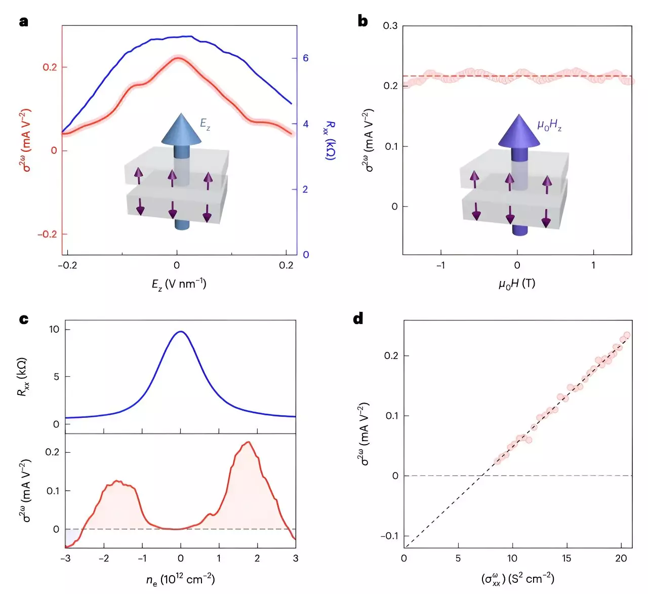
The experiments involved crafting two distinct sets of devices—one utilizing Hall bar electrodes and another comprising radially distributed electrodes—to observe and analyze the current flow. The identification of a nonlinear transport characteristic in both configurations indicated the presence of the antiferromagnetic diode effect, a significant achievement that underscores the material’s unconventional electronic properties.
To scrutinize the underlying phenomena, the team employed a multifaceted approach, incorporating state-of-the-art techniques including spatially resolved optical methods and electrical sum frequency generation (SFG). These methodologies enabled the researchers to observe significant second-harmonic transport patterns, critical for verifying the observation of the antiferromagnetic diode effect. This intricate interplay between experimental design and theoretical prediction illustrates the challenges inherent in studying quantum materials, while also demonstrating the possibilities for uncovering nonlinear electronic responses.
The implications of the antiferromagnetic diode effect extend far beyond academic curiosity, as the researchers themselves posit its critical role in the development of advanced in-plane field-effect transistors and microwave energy harvesting devices. These potential applications may provide substantial benefits in efficiency and performance, marking a vital step towards next-generation electronics that harness the unique properties of antiferromagnetic materials.
Furthermore, the team’s suggestions for utilizing electrical sum-frequency generation as a means to detect nonlinear responses in quantum systems could serve as a valuable tool for future explorations in materials science. This methodology may enable researchers to devise innovative ways to probe and manipulate the unique electronic environments present in complex materials like MnBi2Te4.
The research team’s findings certainly pave the way for a deeper understanding of antiferromagnetic systems and their applicability in contemporary technology. As we stand on the brink of a new era in electronic design, the prospect of integrating antiferromagnetic materials into spintronic circuits becomes increasingly tangible. The potential for developing antiferromagnetic logic circuits and enhancing microwave harvesting capabilities signifies not just an academic success but a tangible contribution to technological evolution.
The work conducted at Harvard opens the door to further studies, encouraging scientists to explore the intricate relationships between quantum materials’ structures, electronic properties, and practical applications. As research in this domain expands, we may expect even more innovative devices that reshape our interactions with technology, pushing the boundaries of what we previously thought possible in electronics.
The antiferromagnetic diode effect discovered in even-layered MnBi2Te4 represents a pivotal advancement in our understanding of antiferromagnetic materials and their role in future technologies. By harnessing the unique properties of these materials, researchers are on the verge of potentially revolutionizing electronic devices, with implications for both consumer electronics and advanced technologies. As investigations continue, the conversation surrounding the intersection of antiferromagnetism and spintronics is likely to intensify, promising exciting developments on the horizon.