
Material science is a continually evolving field that frequently intersects with advanced physics and engineering principles. A significant development in this domain comes from Valery Levitas, an Anson Marston Distinguished Professor of Engineering at Iowa State University, whose recent research reveals groundbreaking findings regarding phase transformations in silicon under unusual conditions. This article explores the implications of this work and its potential applications in technology.
Historical Context and Methodology
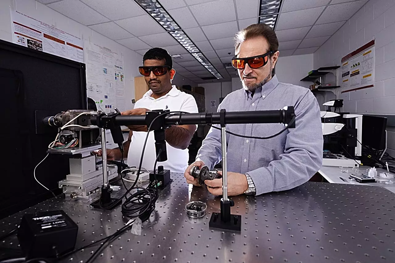
In 1999, Valery Levitas emigrated from Europe to the United States, bringing with him an innovative rotational diamond anvil cell, a tool that has profoundly influenced his research. This apparatus allows scientists to apply extreme pressure and friction to materials, assisting in real-time observations of structural changes at a microscopic level. The research team, under Levitas’s leadership, utilizes this enhanced version of the diamond anvil cell to investigate how various materials behave when subjected to combined pressure and shear forces.
The crux of their investigation revolves around how these pressures affect the microstructural configurations of silicon, a critical component in electronics. Silicon exhibits various crystalline forms or phases, each playing a vital role in its physical properties. Understanding how these crystalline structures transform under low-pressure plastic shear deformation opens up new opportunities for material manipulation that could be game-changing for industrial applications.
The recent study published in Nature Communications sheds light on the previously underexplored realm of silicon’s behavior when subjected to both pressure and shear deformation. The research team discovered that silicon, when manipulated under specific conditions involving particles as small as 100 billionths of a meter, undergoes significant phase transformations at pressures as low as 0.3 gigapascals. This is notably lower than the pressure typically required, which begins at 16.2 gigapascals when pressure alone is applied.
These findings challenge previously held notions within the material science community. They suggest that employing plastic deformations could provide a viable pathway for achieving high-pressure phase characteristics without the impractical logistical challenges of maintaining extreme pressures traditionally associated with such transformations.
For industries relying on silicon—most notably, electronics—the ability to manipulate silicon’s crystalline phases under much lower pressures is monumental. The possibility of retrieving nanostructured pure phases or mixtures (nanocomposites) with optimized electronic, optical, and mechanical properties is set to revolutionize the way semiconductor materials are developed and utilized.
Levitas emphasizes that the real goal of their team’s research is not simply to alter the size or shape of materials but to induce changes in microstructure. These minute adjustments can yield significant variations in properties, which may otherwise remain unattainable with conventional high-pressure methods. The understanding that unique phase transformations can occur even at relatively low pressures expands the toolkit available to engineers and researchers alike.
Future Directions and Sustained Research
The revelations from this study represent not just a single breakthrough but a stepping stone for further exploration in the field of material science. Levitas admits that had they not anticipated phase transformations at lower pressures, they would never have investigated this area. This mindset underscores the necessity for continued research and experimentation, as it is often the unexpected outcomes that lead to the most transformative advancements.
With ongoing investigations into silicon and its various phases, researchers aim to refine the techniques used in applying plastic deformation and pressure. As industries look to innovate, the findings promise a transformative impact on how materials are engineered, with potential applications reaching far beyond basic silicon manipulation.
Levitas and his team’s pioneering work offers a glimpse into the future of material science, where the fusion of advanced mechanics, physics, and engineering propels the field toward unprecedented discoveries and applications. The ability to adapt and innovate in material manipulation heralds a new era for technological advancement in sectors heavily reliant on silicon, embodying a level of interdisciplinary cooperation that is vital for tackling future challenges in the field.