
Electronic devices have come a long way in terms of performance and efficiency, but there are still limitations to be overcome. Electronics engineers and materials scientists are constantly on the lookout for new materials that can push the boundaries of current technology. One promising candidate that has caught the attention of researchers is two-dimensional (2D) semiconductors.
2D semiconductors offer a range of advantageous properties that make them stand out from traditional silicon-based transistors. One key advantage is their atomic thickness, which can lead to improvements in electrostatic control and transistor performance. Additionally, 2D semiconductors exhibit high carrier mobilities, which can further enhance their performance in short-channel field-effect transistors (FETs).
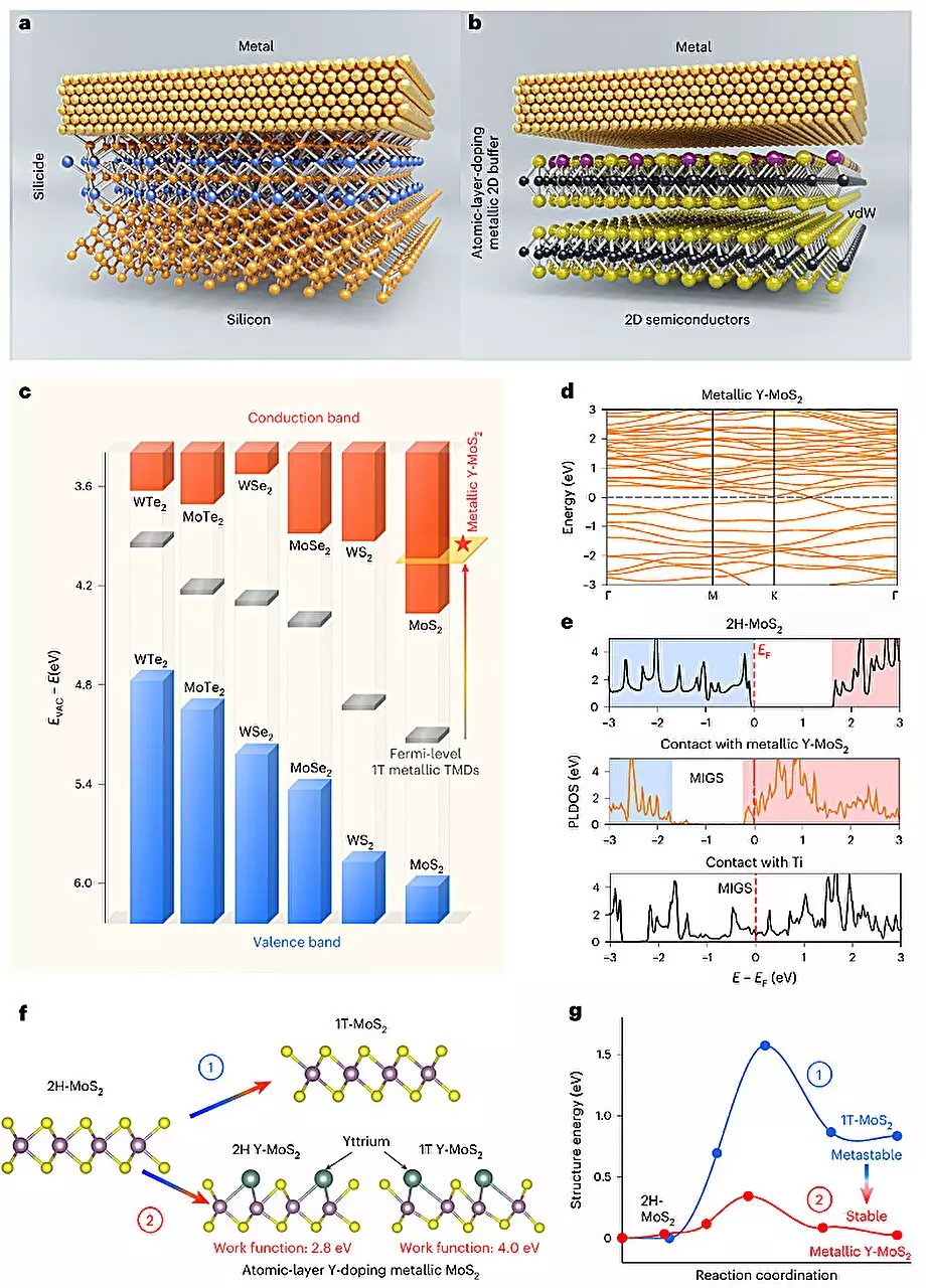
Despite their promise, 2D semiconductors still face challenges, particularly in terms of high contact resistances due to Fermi-level-pinning effects. These limitations have hindered their integration into electronics on a large scale. However, researchers at Peking University and Chinese Academy of Sciences have introduced a new yttrium-doping strategy that could potentially address this key limitation.
The Yttrium-Doping Strategy
The new yttrium-doping strategy involves converting semiconducting molybdenum disulfide (MoS2) into metallic MoS2. By introducing a semi-metal layer between a metal electrode and the 2D semiconductor, researchers were able to enhance the efficiency of carrier injection. This strategy draws inspiration from the traditional silicide structure used in silicon-based transistors.
To achieve yttrium doping in MoS2, researchers developed the plasma-deposition-annealing (PDA) method. This involved treating patterned local contact areas with low-power soft plasma to generate active sites, followed by the deposition of a Y/Ti/Au stacked metal. The Y atoms then diffuse into the active sites and are activated through high-temperature annealing in an inert gas environment.
The 2D Phase Transition
The researchers introduced the concept of a “rare earth element yttrium doping-induced 2D phase transition” in their paper. This phase transition essentially refers to the metallization observed when applying the yttrium-doping strategy to MoS2. This breakthrough allows for the doping depth to be pushed to the atomic layer limit of 0.5 nanometers, overcoming traditional engineering limitations.
Future Implications
Using the yttrium-doping strategy, researchers were able to develop ultra-short MoS2-based channel ballistic transistors with excellent performance as ohmic contacts and switching capabilities. These transistors hold promise for the development of new sub-1 nanometer node chips that can achieve remarkable performance while consuming less power than conventional chips. The researchers are now focusing on developing equally excellent p-type ohmic contacts suitable for 2D semiconductors.
The introduction of yttrium-doped 2D semiconductors represents a significant step towards overcoming the limitations of current electronics. By addressing key challenges such as high contact resistances and Fermi-level-pinning effects, researchers are paving the way for the development of more efficient and high-performing electronic devices. With further advancements in this field, the future of electronics looks bright and promising.