
In a groundbreaking development in semiconductor research, scientists at UC Santa Barbara have successfully captured the first visual representation of electric charges moving across the interface of two distinct semiconductor materials. The research findings, published in the Proceedings of the National Academy of Sciences, reveal the remarkable dynamics of photocarriers, which are integral to the functionality of various electronic devices including solar cells and lasers. This research not only advances our understanding of charge carrier behavior but also serves as a conduit for refining existing semiconductor theories and practices.
Historically, while a plethora of theories and indirect measurements have explained the complexities of charge movement within semiconductor materials, the ability to directly observe these phenomena in real-time has been limited. Liao, an associate professor of mechanical engineering, expressed that the research team’s work allows for the visualization of processes that have long been relegated to theoretical discussions. The advent of scanning ultrafast electron microscopy (SUEM) techniques marks a significant step forward, as it enables researchers to witness the microcosmic dance of charges as they traverse semiconductor boundaries.
This direct observation is a key milestone for semiconductor materials science, providing a tangible means for researchers to validate theoretical frameworks and understand the behavior of these entities at the nanoscale. The knowledge gleaned from this research could play a transformative role across a variety of applications, from enhancing energy efficiency in photovoltaics to optimizing performance in semiconductor devices.
The mechanism underlying photocarrier production is fundamentally simple: when sunlight strikes a semiconductor, it energizes electrons, prompting them to move and create an electric current. However, the intricacies of their movement can have profound implications for energy conversion and device performance. It is crucial to monitor how these photocarriers operate right after their initial excitation, particularly since they lose a significant portion of their energy within picoseconds, transitioning to a “cooler” state that is less efficient for energy capture.
Through the lens of Liao’s research, one major focus is on the behavior of “hot” photocarriers, whose energetic state holds untapped potential for improving energy efficiency. As these carriers migrate across semiconductor interfaces—known as heterojunctions—they face challenges such as energy loss in the form of heat, which directly impacts overall device performance. Understanding the movement of these charges at the heterojunction level is vital, as it can lead to the design of materials that mitigate energy loss and enhance conductive properties.
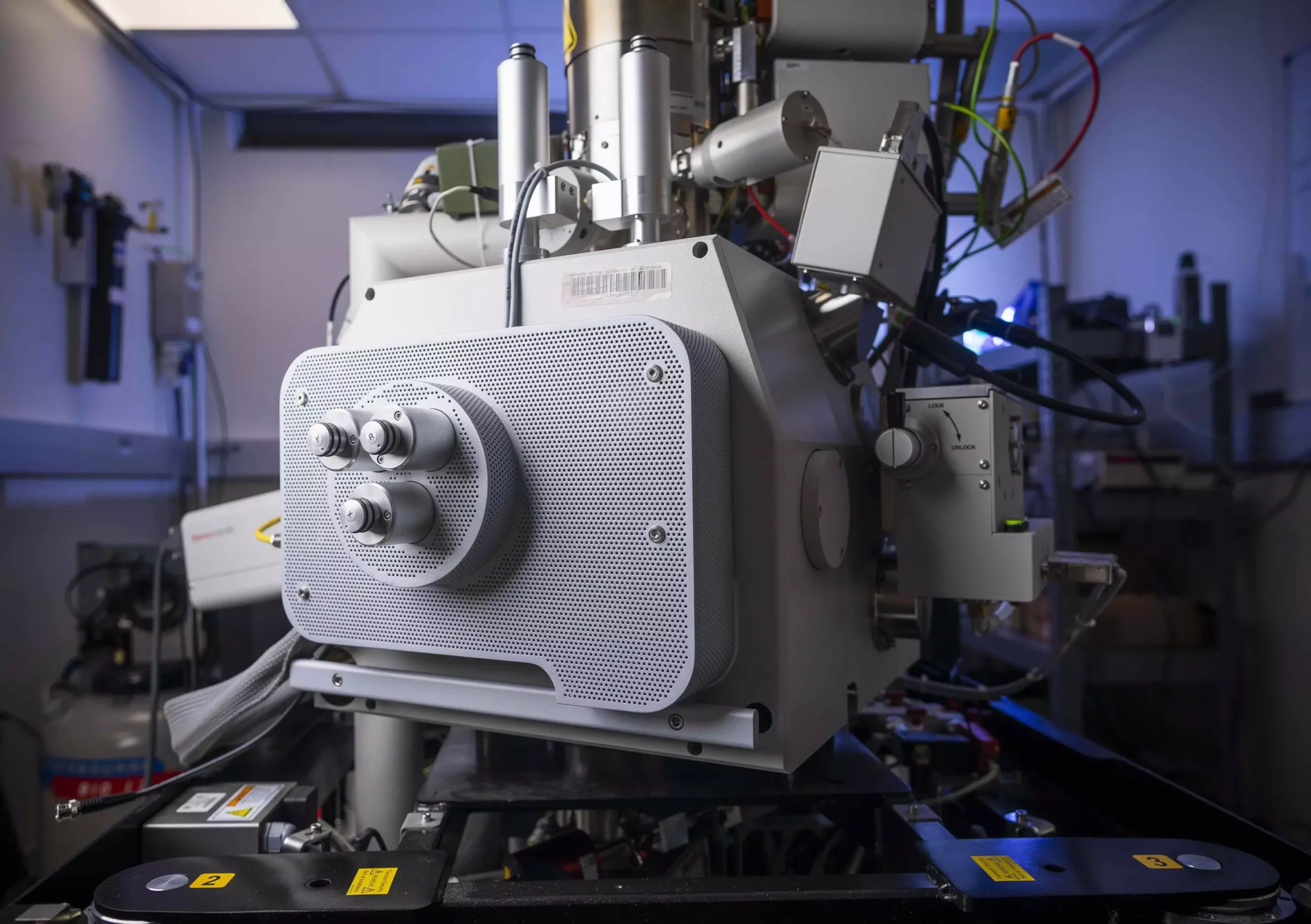
The methodology employed by the research team integrates ultrafast laser pulses with SUEM techniques, creating a unique imaging system capable of capturing events unfolding within the scale of picoseconds to nanoseconds. By synchronizing an electron beam with rapid laser activities, researchers can achieve unprecedented temporal resolution, essential for visualizing the transient states of charge carriers as they migrate from one semiconductor to another.
The findings from this research illustrate how these hot carriers behave when generated in uniform silicon or germanium regions compared to their behavior near a heterojunction. Specifically, while photocarriers in uniform regions exhibit rapid movement, those excited near the junction may experience trapping, significantly reducing their mobility and thus impeding device efficiency. This illumination of charge carrier dynamics at the heterojunction has important ramifications for future semiconductor device design and optimization.
The current research underscores a legacy of semiconductor innovation at UC Santa Barbara, harking back to the contributions of Herb Kroemer, a pioneer in the development of heterostructures. Kroemer’s assertion that “the interface is the device” laid the groundwork for much of modern information technology. By bringing Liao’s contemporary findings into the discourse, the university continues to foster advancements that build upon foundational semiconductor theories.
The capability to visualize these hot carrier activities opens new avenues for practical applications and theoretical insights within the semiconductor field. As researchers continue to explore the interactions and behaviors at semiconductor interfaces, the evolving landscape of technology may soon witness fundamentally improved devices that capitalize on the hot carrier phenomenon.
As we continue to unlock the mysteries of charge carrier behavior in semiconductors, the implications of this research extend far beyond the confines of academic inquiry. The direct visualization of hot photocarriers introduces a novel paradigm that has the potential to reshape how semiconductor devices are conceived and constructed. Moving forward, understanding and harnessing these fleeting phenomena may lead to significant advances in energy capture, telecommunications, and electronic device performance, solidifying the indispensable role of semiconductor research in our technologically driven world.